
Info 1: Behind the scene of MEMS
Are we not all fascinated by the craftsmanship of the Swiss watchmakers − creating high precision systems so small that magnifiers are needed during assembly? Today, there is a need for even smaller devices.
MEMS involves a multitude of materials and processes. The complexity of MEMS can range from simple mechanical structures to completely miniaturized fluidic multifunctional systems containing actuators, sensors and electronics. The opportunities are limited only by imagination.
Opportunities
MEMS has matured and the technology push is now complemented by a multibillion dollar market pull. There are now specialized foundry companies that focus on manufacturing customer-designed MEMS chips and components. A specialized sensor industry based on small to medium-sized companies has evolved. A few large companies in the semiconductor and automotive areas have invested in their own MEMS facilities.

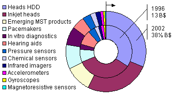
Market forecast made by NEXUS in 1998.
MEMS-based components are used in many applications such as medical, automotive, telecommunication, IT and space. Typical mass-produced examples are:
- Accelerometers for airbag systems
- Chemical and pressure sensors for medical applications
- Heads for ink jet printers and hard disk drivers
- Quartz watch crystals resonators for time-keeping
The automotive field was the MEMS leader in the early 1990s. Its importance is less dominating today due to the rapid growth in other MEMS fields. Characteristics of the automotive industry are few suppliers, large quantities, tough cost-pressure, high quality requirements, and harsh environments.
Factors influencing the use of MEMS in the medical field are mainly the drive to reduce costs and sample size, to speed up analyses, and the need to prevent faulty diagnosis and treatment. A reduced cost opens new markets such as tests done at home using smart phones. Examples of application include diagnostic and drug delivery systems for clinical and home use, lab-on-chip, hearing aids, pacemakers and minimally invasive surgery.
There are several interesting IT-related applications including optical switches and other components for the broadband net and mirror arrays for projectors. A strong trend is that MEMS components have found their way into smart phones.
Processes

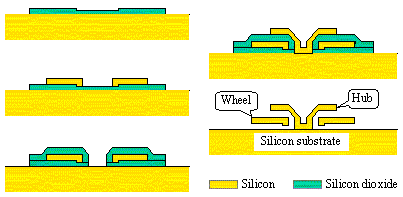
This cross-section sequence shows how a free-floating wheel can be created using deposition and selective etching.
Micromachining has, since its introduction in the 1960s, developed its own arsenal of fabrication tools based on processes similar to those developed for the semiconductor industry. Its toolbox now contains many powerful tools based on etching, deposition and bonding. Some characteristics are:
- The size of the fabricated structures range from sub-micrometer for the smallest details up to several millimeters for complex devices and systems.
- The first production steps are performed on a wafer level. This enables batch production in which a large number of identical devices are manufactured simultaneously.
- Wet and dry etching is often used to remove material and to sculpture detailed features. Crystalline materials are anisotropic which result in a complex dependence of the etch speed on material, etch direction, etchant and temperature (selective etching).
- Thin films of various materials, characteristics and thickness can be depositing on the surface. Free-floating structures can be created by etching away thin embedded sacrificial layers (see figure).
- Joining of pieces (bonding) is often done without conventional adhesives. Anodic bonding uses a very thin intermediate layer (e.g. glass) that is melted at high temperature, while silicon-to-silicon fusion bonding does not rely on any intermediate material at all. Bonding is often done on a wafer level, and can be used to create cavities, to package the sensor chips, etc.
- Patterning is done with various masking techniques (photolithography) that often involve covering selected areas with materials, such as photoresist and oxide, that are resistant to the liquid etchant or to the particle bombardment encountered in dry etching.
- Combining etching, deposition and bonding makes it possible to form complex three-dimensional structures and complete sensor systems that can include several MEMS materials.
- For some micromachining materials, such as silicon, it is possible to integrate electronics onto the same chip as the sensor element.
Micromachining comes in two varieties, bulk and surface micromachining (BM and SM). Both date back to the 1960's, and were developed in parallel. Although some process steps are common for both, there are notable differences. Combinations of the two techniques exist. Both BM and SM are commonly used for silicon while BM is the predominant technique used for quartz.
BM tailors the substrate wafer itself into the desired geometric shape, while SM is based on deposition and etching of thin layers on one side of the wafer. With SM it is difficult to create thicker structures, while both thick and thin structures can be formed with BM. SM often generates free-floating layers that curve due to the thermal stress caused by the mismatch in thermal expansion coefficients between the deposited materials and that the films often are deposited at elevated temperatures.
The material selectivity during etching is essential for SM in the same way as BM relies on the anisotropy of the etching. Both BM and SM use ordinary photolithographic methods for patterning the shapes. In general, SM is more compatible with electronics and enables freely movable structures, but it often involves more complex process steps.
Materials
System requirements vary with application. To best succeed, one should let the requirements govern which of the many complementing MEMS materials one choose.
The most common material for micromachining is, just as for semiconductors, silicon. Although not always the best material, it is a general and flexible material that can be used for a large number of components. This has made silicon a natural choice for some large companies that focus on a broad range of MEMS based products, which, in its turn, has influenced universities and financiers to focus less on alternative materials. The investment in know-how and production equipment creates an inertia that further strengthens silicon's dominance.
Both single and poly-crystalline silicon are used. Crystalline silicon has anisotropic etch properties which allows the creation of geometries with features such as vertical walls and thin membranes using wet etching. Examples of sensors that successfully use the silicon technology are pressure sensors for medical applications and accelerometers for airbag systems. For silicon, the excitation of vibrations and deflections is often done electrostatically, thermally or magnetically, and the detection capacitively or via the stress-dependence of piezoresistors (silicon is not piezoelectric).
GaAs is another micromachinable semiconductor material that is of interest for niche applications. It is mainly its optical properties that attract attention.

The most successful micromachined product, the watch crystal tuning fork, is based on quartz (crystalline SiO2). Quartz's piezoelectric effect, inertness, and excellent temperature stability and aging properties make it the unsurpassed choice for this application. Micromachined watch crystals are manufactured in six-digit quantities each hour at a production cost of less than $0.20 a piece, including package and individual laser trimming. High performance MHz resonators, accelerometers and chemical sensors are other niche applications for which micromachined quartz is used successfully. Its high-yield process steps have been developed mainly by the watch crystal industry. Only a few universities include quartz in their research programs.
Polymeric microstructures offer an interesting alternative that can lead to cost savings on the order of 100 to 1000 times when the MEMS components are large as they are for, for example, lab-on-chip applications. The structures are produced by a microreplication technique similar to that used to create CD discs. The master is created using conventional micromachining and MEMS-materials. Several replicated polymeric MEMS products are available on the market today, particularly for microfluidic platforms and in consumer and low-cost disposable applications.
Additional promising materials are being explored for MEMS, such as metals and diamond.
