
Info 2: MEMS-related Words
The following contains words you might encounter when talking to MEMS people, but might have hesitated to ask what they mean.
Actuator: Device converting energy (electric, chemical, etc.) into mechanical work.

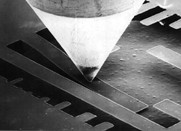
AFM: Atomic Force Microscopy. Visualizes features on an atomic scale.
Anisotropic etching: Direction-dependent etching. Often based on the periodic order of crystalline materials (anisotropy).
Anisotropy: Different material or processing properties in different directions.
Anodic (field-assisted) bonding: Bonding conductive to non-conductive materials (e.g. silicon to glass) using heat and high-voltage-generated electrostatic forces.
ASIC: Application-Specific Integrated Circuit. En electronic chip specially designed for a certain customer and application.
Batch: Production of many components at the same time.
Bonding: Joining of parts in a permanent way.
Bulk micromachining: Tailoring structures by machining a wafer's interior.
Cleanroom: Ultra-clean area with a controlled environment.
CMOS: Complementary Metal Oxide Semiconductor. Type of integrated electronics often used in one-chip solutions.
CVD: Chemical Vapor Deposition. Deposition of thin layers on the surface through chemical reactions.
Dielectric material: A non-conducting material.
Direct wafer bonding: Bonding wafers without using an intermediate adhesive material.
Dry etching: Processes based on chemically aggressive gases (e.g. RIE), plasma, and particle-bombardment.
EDM: Electro Discharge Machining. Milling using electric sparks.
EDP: Ethylene Diamine Pyrocatechol. An alternative to KOH for wet etching of silicon.
Electroplate: Deposition of metals using an electric current and an electrolyte solution.
Electrostatic force: Mechanical force caused by a voltage difference between two electrodes.
Epitaxy: Atom by atom growth of layers that adjust to the crystallographic orientation of the substrate (a single crystal).
Etch stop: Technique of stopping the etching at well-defined locations, e.g. at silicon-insulator interfaces or P-N junctions in semiconductors.
Etching: Removal of material, often with chemical processes.
Evaporation: Deposition using a heated source that sublimate or boil. Low pressure ensures high directionality of the vapor condensing at the substrate.

Fab: Factory for microstructures (nickname similar to lab).
FEA/FEM: Finite Element Analysis and Method. Simulation procedure for analyzing multiphysics behavior.
FIB: Focused Ion Beam. Finely focused ion beam (often Ga+) used for imaging, milling and deposition.
Fused silica: Non-crystalline (amorphous) quartz.
GaAs: Gallium Arsenide. Semiconductor with optical and piezoelectric properties.
HF: Hydrofluoric acid. Ingredient in etchants that attack SiO2 (incl. quartz).
Hydrophilic: A drop of water will wet a hydrophilic surface.
Hydrophobic: The opposite to hydrophilic.
Isotropic etching: Direction-independent etch speed.
KOH: Potassium Hydroxide. A common etchant for wet etching of silicon.
LCVD: Laser-assisted CVD.
LIGA: Lithographie, Galvanoformung, Abformung. Synchrotron radiation is used to form high-aspect ratio polymeric structures suitable for metal filling by electrodeposition and as masters for replication.
Lithography: Copying a mask-pattern onto a surface, e.g. using light or X-ray.
Lorentz force: Mechanical force caused by an electric current in a magnetic field.
LPCVD: Low Pressure CVD.
Mask: Pattern to be copied with etching or deposition.
MCM: Multi Chip Module.
MEMS: MicroElectroMechanical System. See 'Microsystem' and 'MST'. Acronym originally used primarily in the USA. Used today in most parts of the world.
Micromachine: See MST. Word primarily used in Asia.
Micromachining: Processes for microstructure fabrication. Originating from the semiconductor industry's processes.
Microstructure: Structure featuring small geometries (sub-µm to mm). Often fabricated using micromachining.
Microsystem: System including one or more microstructures or assembled using microtechnology.

µ-TAS: Miniaturized Total Analysis System. Integrated chemical sensor system.
MOEMS: MicroOptoElectroMechanical System.
MPW: Multi Project Wafer. Several projects share the space and cost of a wafer.
MSB: Micro Structure Bulletin. Nordic MEMS newsletter published in 1993-1999.
MSK: MikroStrukturKurs. Swedish MEMS course first held in 1994.
MST: MicroSystem Technology (regionally also MicroStructure Technology). See 'Microsystem'. Acronym originally used in Europe but is now often replaced with 'MEMS'.

MSW: Micro Structure Workshop. Nordic biennial MEMS workshop first held in 1994.
OEM: Original Equipment Manufacturers sell to system manufacturers instead of directly to customers.
One-chip solution: Sensor element and its electronics integrated on one chip.
Photoresist: Substance used to protect areas not to be etched. Patterned via lithography followed by removal (etching) of exposed (or unexposed) areas.
Piezoelectricity: Mechanical stress generated by electric field/charge, and vice versa. Present in strongly anisotropic dielectrics, e.g. quartz.
Piezoresistance: The dependence of resistivity on mechanical stress. Involves mainly semiconductors, e.g. silicon.
Plasma: Cloud of ionized gas and electrons.
Polysilicon: Silicon consisting of crystalline grains. Often deposited via CVD or PVD.
PVD: Physical Vapor Deposition. Deposition processes such as sputtering and evaporation.
PZT: Lead Zirconate Titanate. Large-strain piezoelectric ceramic.

Quartz glass: See fused silica.
Quartz: Crystalline SiO2. An inert, highly stable, and piezoelectric material. Used, for example, for tuning fork watch crystals.
Resonator: Mechanical structure that vibrates, sometimes at a resonance frequency.
RIE: Reactive Ion Etching. Dry etching based on plasma with chemically active gas ions.
Sacrificial layer etching: Removal of a buried fast-etching layer used, for example, to create freely movable structures.
SEM: Scanning Electron Microscopy. Features too small for optical microscopy made visible by scanning the sample with an electron beam.
Sensor: Device providing useful output to a specified stimulus. May react also to other stimuli, e.g. temperature.
Silicon fusion bonding: High-temperature hermetic bonding. Its atomic nature means high-quality bond interfaces.
Silicon: The most popular material in micromachining.
SME: Small to Medium-sized Enterprise (company).
SOI: Silicon On Insulator. An oxide layer sandwiched between two silicon layers, used in etching as an etch stop barrier and sacrificial layer.
Sputtering: Deposition based on bombarding a source by ions from a gas plasma. Knocked out atoms lose their directionality when passing through the plasma on their way to the substrate.
Stiction: Undesired adhesion of movable solids in very close proximity, caused by forces such as Van der Waals, capillary and hydrogen bridging.
Surface micromachining: Forming structures via deposition and etching of thin layers on the wafers surface.
TEM: Transmission Electron Microscopy. Visualizes details in thin slices via the transmission of an electron beam.
Transducer: Device, e.g. sensor or actuator, converting energy from one domain to another, calibrated to minimize conversion errors.
Wafer: Thin slice of material suitable for batch processing. Normally circular with diameters in the 50-300 mm range.
Wet etching: Etching using chemically aggressive liquids.
Wire bonding: Making electrical connection by attaching thin gold or aluminum wires.
Yield: Fraction of functioning components after processing.
(Excerpt from Micro Structure Bulletin − MSB 99:4 ©)
